
Single Phase Semi-Converter with R Load, RL Load and RLE Load
Introduction
Single phase fully controlled bridge converters are two quadrant converters having unidirectional
current with both positive and negative voltage polarity. Thus they can be operated either as a
controlled rectifier or an inverter. But for some applications that do not utilize the inverter mode
operation, a fully controlled converter with four thyristors and their associated control and gate drive
circuit makes the system unnecessarily complicated. In such situations, two of the thyristors of a
single phase fully controlled converter has to be replaced by diodes. The resulting
converters are called single phase semi-converter or single phase half controlled converters. Semi-convertors
are single
quadrant converters having one polarity of voltage and current at the DC terminals.
1. Single Phase Semi-Converter - R Load
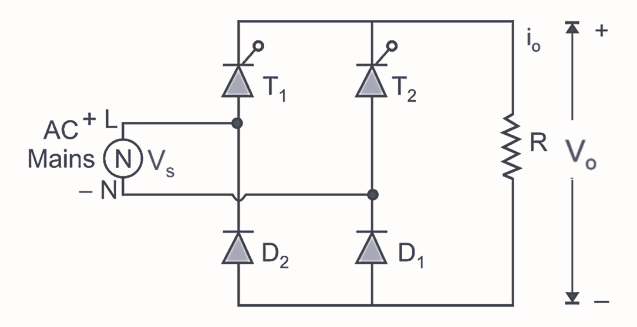
In the figure, shows the circuit diagram of single phase semiconverter bridge rectifier with R load. In this
rectifier two SCRs and two diodes are connected in symmetrical configuration. The operation of this converter mainly consists of three modes:
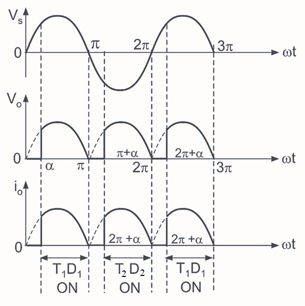
Mode 1: (α to π)
During positive half-cycle of AC input voltage, thyristor T1 diode D1 conduct and
thyristor T1 is fired at ωt = α. Therefore the average output voltage is equal to the
instantaneous supply
voltage and load current flows through T1, R, D1 and back supply again.
Mode 2: (π to π + α)
At instant ωt = π, the supply goes through zero and after π supply voltage reverses its polarity. Due to
reverse supply across conducting devices T1 and D1, they turned off at ωt = π and this
type
of turn-off is called as "natural" or "line commutation". Therefore, the average output voltage is zero and
load current is also zero.
Mode 3: (π + α to 2π)
At instant ωt = π + α, the supply voltage becomes completely negative i.e., during negative half cycle of
AC input voltage, thyristor T2 and diode D2 are forward biased, thyristor T2
is fired at ωt = π + α.
Thus the average output is equal to instantaneous supply voltage because due to conduction of T2
and D2, the load is directly connected to supply. The load current flows through T2, R,
D2. Thyristor T2 and diode D2 conduct upto
2π, at ωt = 2π commutation takes place due to natural zero appears across supply.
The average and rms value of output voltage and current are,
$$V_{o} = \frac {V_{m}}{\pi}( 1 + cos\alpha ) .......(1)$$
$$I_{o} = \frac {V_{o}}{R} = \frac {V_{m}}{\pi R} ( 1+ \cos\alpha).......(2)$$
$$V_{o~(rms)} = \frac {V_{m}}{\sqrt {2}} \left[ \frac {1}{\pi}\left(\pi - \alpha + \frac {sin 2\alpha}{2}\right) \right]^{\frac {1}{2}}.......(3)$$
$$I_{o ~ rms} = \frac {V_{o ~ rms}}{R} = \frac {V_{m}}{\sqrt {2} R} \left[\frac {1}{\pi}\left(\pi - \alpha + \frac {sin 2\alpha}{2}\right) \right]^{\frac {1}{2}}.......(4)$$
2. Single Phase Semi-Converter - RL Load with Freewheeling Diode
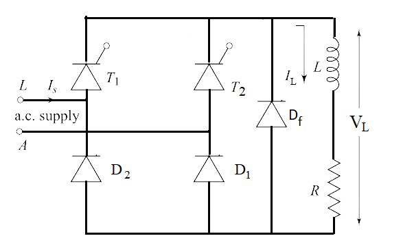
Due to inductive load, there will be a flow of load current even after phase reversal i.e., after completing
each half cycle. This is because, due to the large inductive nature of the load, the load current has a
tendency to flow continuously by finding an alternative path through the diode of the same arm of conducting
SCR even after phase reversal. Thus, there will be no control over the thyristor once it is triggered as seen
in continuous and discontinuous modes.
This problem can be overcome by connecting a diode in parallel with the load. This diode is known as a fly-back diode or freewheeling diode. When there is a phase reversal, this diode acts as the short-circuit path for inductive load current rather than passing it through the thyristors. Hence, The thyristor regains its blocking state once there is a phase reversal in the supply.
The free-wheeling diode improves the load current waveform and increases the input power factor. It also eliminates the damage of the current components from the formation of voltage spikes during the turn-off period of the thyristors and diodes.
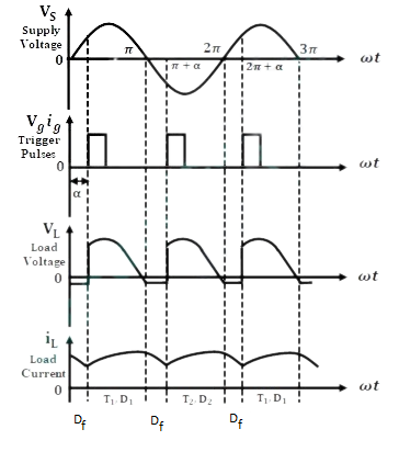
In this circuit, at ωt = π, T1 and D1 become reverse biased, whereas the freewheeling diode Df becomes forward biased. Hence, after ωt = π, the load current will be transferred from T1 D1 to Df. Now the current flows through the path Df, R, L and then Df. During this period, the output gets short circulated through Df and the output voltage will be zero as shown in the below waveforms.
This process continues from π to π + α. When T2 is triggered at ωt = π + a, D2 and Df get forward biased. Now the load current shifts from Df to T2 D2, and again the load voltage follows the supply voltage till ωt = 2π. At ωt = 2π, T2 and D2 get reverse biased, and Df gets forward biased, and again the above process repeats.
We can see that the above load current and load voltage waveforms are similar to the waveforms of the converter without a freewheeling diode. But here load current due to inductive load is transferred back to it through the freewheeling diode Df rather than through the thyristor and diode combination T1 D2 and T2 D1. Hence the freewheeling diode improves the circuit performance and also ensures commutation of thyristors at the end of each half-cycle providing a controlled load current under the triggering circuit.
The average and rms of bridge output voltage are,
$$V_o = \frac {2}{2\pi} \int_{\alpha}^{\pi} V_{m}sinwt ~ dwt = \frac {2V_m}{2\pi}\big[-cos\omega t \big]_{\alpha}^{\pi} = \frac {V_m}{\pi}(1 + cos\alpha).......(5)$$
$$V_{o~(rms)} = \left[ \frac {2}{2\pi} \int_{\alpha}^{\pi} V_{m}^2 ~ sin^2wt ~ dwt \right]^{\frac {1}{2}}.......(6)$$
$$V_{o~(rms)} = \left[ \frac {V_{m}^{2}}{2\pi} \int_{\alpha}^{\pi} (1 - cos2\omega t) ~ dwt\right]^{\frac {1}{2}}.......(7)$$
$$V_{o~(rms)} = \frac {V_{m}}{\sqrt {2}} \left[ \frac {1}{\pi}\left(\pi - \alpha + \frac {sin 2\alpha}{2}\right) \right]^{\frac {1}{2}}.......(8)$$
3. Single Phase Semi-converter - RLE Load with Freewheeling Diode
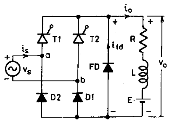
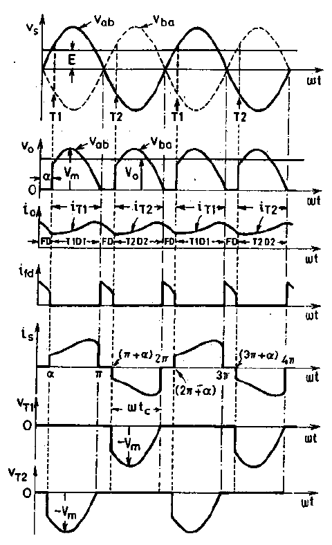
The circuit consists of two thyristors, two diodes, and a freewheeling diode across the load. After
ωt = 0, thyristor T1 is forward biased only when source voltage Vm sin ωt exceeds E.
Thus, T1 is triggered at a firing angle delay α such that Vmsinα > E. With
T1 on, load gets connected to source through T1 and D1. For the period
ωt = α to π, load current io flows through RLE, D1, source and T1 and
the load terminal voltage vo is of the same waveshape as the ac source voltage vs. Soon
after ωt = π, load voltage vo tends to reverse as the ac source voltage changes polarity. Just as
vo tends to reverse, FD is forward biased and starts conducting. The load current io is
transferred from T1, D1 to FD. As SCR T1 is reverse biased at ωt > π through
FD, therefore load voltage vo is zero during π < ωt < (π + α). After ωt = π, during
the negative half cycle, T2 will be forward biased only when source voltage is more than E. At ωt
= π + α, source voltage exceeds E, T2 is therefore triggered. Soon after (π+α),
FD is reverse biased and is therefore turned off; load current now shifts from FD to T2,
D2. At ωt = 2π, FD is again forward biased and output current io is transferred from
T2, D2 to FD as explained before.
The average and rms of bridge output voltage are,
$$V_o = \frac {2}{2\pi} \int_{\alpha}^{\pi} V_{m} ~ sinwt ~ dwt = \frac {2V_m}{2\pi}\big[-cos\omega t \big]_{\alpha}^{\pi} = \frac {V_m}{\pi}(1 + cos\alpha).......(9)$$
$$V_{o~(rms)} = \left[ \frac {2}{2\pi} \int_{\alpha}^{\pi} V_{m}^2 ~ sin^2wt ~ dwt \right]^{\frac {1}{2}}.......(10)$$
$$V_{o~(rms)} = \left[ \frac {V_{m}^{2}}{2\pi} \int_{\alpha}^{\pi} (1 - cos2\omega t) ~ dwt\right]^{\frac {1}{2}}.......(11)$$
$$V_{o~(rms)} = \frac {V_{m}}{\sqrt {2}} \left[ \frac {1}{\pi}\left(\pi - \alpha + \frac {sin 2\alpha}{2}\right) \right]^{\frac {1}{2}}.......(12)$$
Advantages of Single Phase Semi-converter
Single-phase semiconverters have a straightforward design with fewer components compared to three-phase converters. This simplicity makes them cost-effective and easier to implement, particularly for low-power applications.
Due to their simpler design, single-phase semiconverters tend to be more compact, making them suitable for space-constrained applications or when a compact form factor is essential.
Controlling single-phase semiconverters is less complex compared to three-phase converters. The control circuitry is simpler, leading to reduced development and maintenance costs.
Single-phase semiconverters find applications in various industries, including small motor drives, battery chargers, uninterruptible power supplies (UPS), and household appliances like laptops, mobile phone chargers, and small electronic devices.
By varying the firing angle of the semiconductor switches (such as thyristors or silicon-controlled rectifiers), the output voltage can be controlled effectively. This feature allows for regulation of the output DC voltage, making it suitable for applications where variable voltage control is required.
In regions or applications where only single-phase AC power is available, single-phase semiconverters become the obvious choice for converting AC to DC.
Disadvantages of Single Phase Semi-converter
Compared to three-phase converters, single-phase semiconverters have relatively lower efficiency due to the pulsating nature of the output current. Three-phase converters offer smoother output and therefore higher efficiency.
Single-phase semiconverters are generally limited to lower power applications. For high-power applications, three-phase converters are preferred as they distribute the power more evenly and efficiently.
The pulsating nature of the output current in single-phase semiconverters can lead to higher harmonic content in the AC supply, potentially causing issues with power quality and electromagnetic interference.
Applications of Single Phase Semi-converter
High power converters
Main line a.c. traction
Electroplating
Battery Charging Systems
Static VAR systems